Question: Consider the inverter below. When the input VI is high, the switch is closed, and when the input is low, the switch is open. Assume the input is a 5-V TTL pulse with duration T. Assume that capacitor is fully charged for t<0.RD=1kΩ;Ron=250Ω;CL=0.25pF. The circuit is based on the NMOS inverter logic discussed in the class, where capacitor
Consider the inverter below. When the input high, the switch closed, and when the input low, the switch open. Assume the input pulse with duration Assume that capacitor fully charged for ;; The circuit based the NMOS inverter logic discussed the class, where capacitor discharges defined the MOSFET parameters and values.For and the time range the plot should coverGive approximate sketch the output pulse forGive approximate sketch the output pulse forComment the level distortion due transmission for each pulse duration.Determine the propagation delay due the inverter circuit.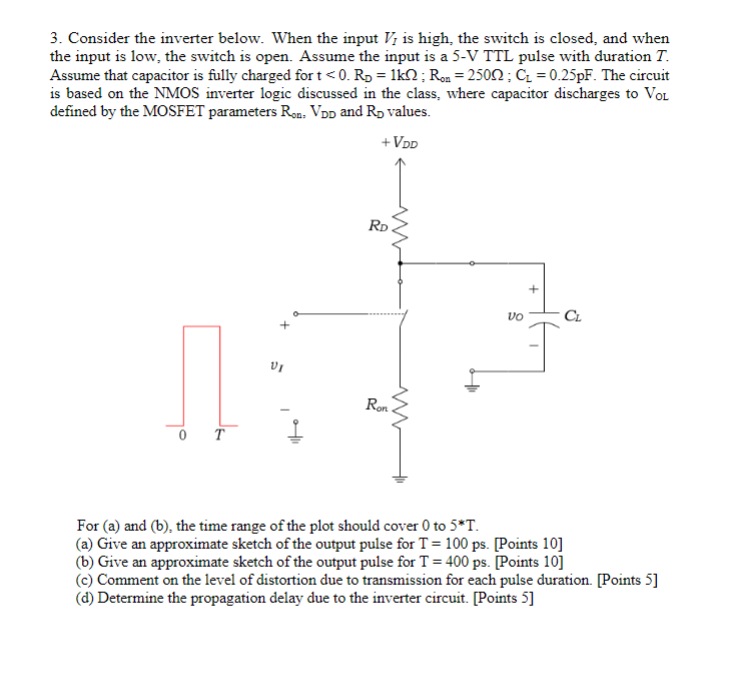
 This question hasn't been solved yet!Not what you’re looking for?Submit your question to a subject-matter expert.
Not the question you’re looking for?
Post any question and get expert help quickly.